The Cortex Bridge (the 0AMS bridge, revision A4) connects to the Klipper host by USB on one side. On the other side it connects to the AMS RS-485 network and supplies 24 V. The AMS units keep their stock firmware. This page names every part you can see on the board and says which parts are unused or not fitted.
¶ Board views
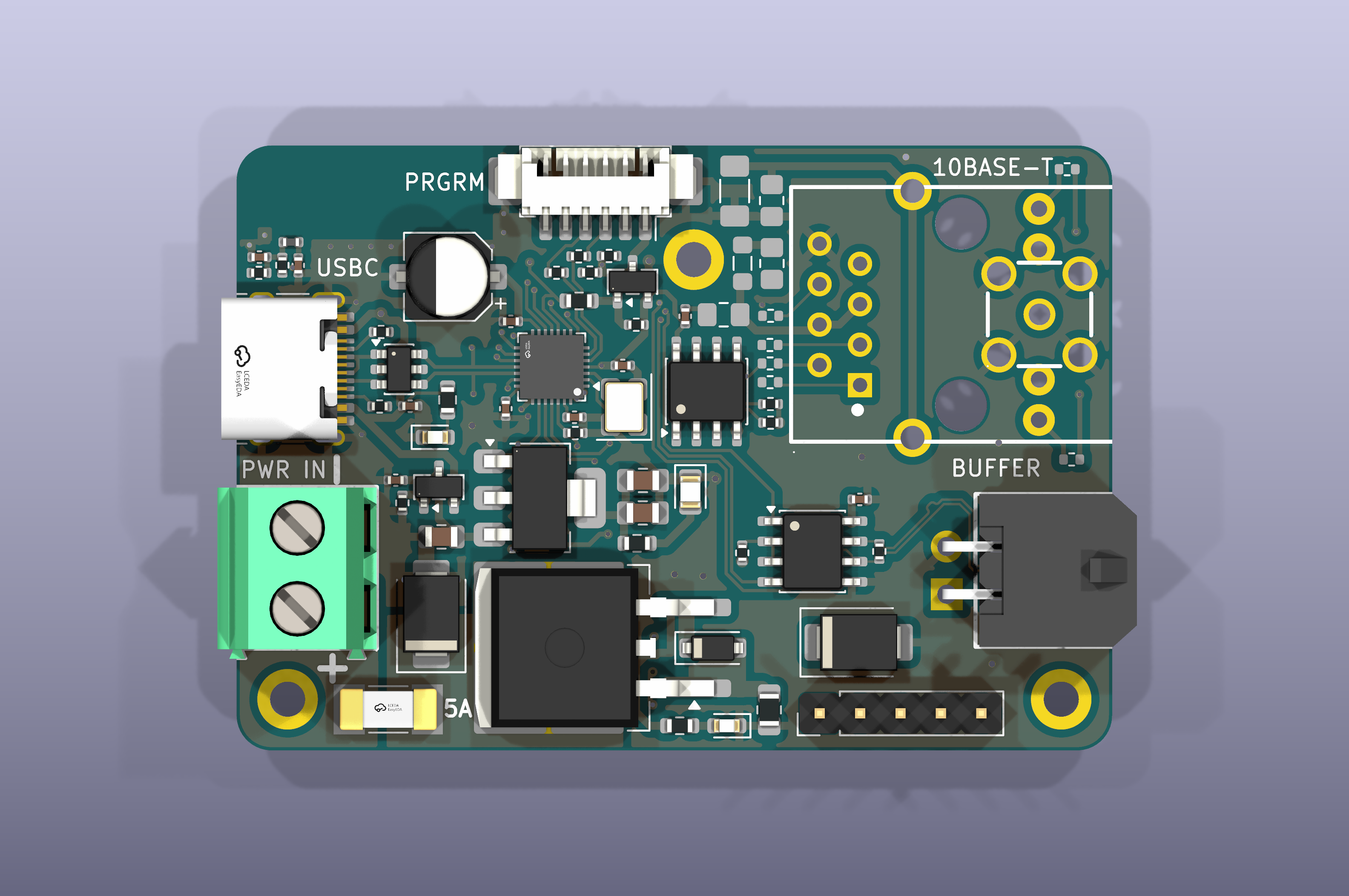
Component side. The USB-C connector (J1) is at the left, and the PWR IN screw terminal (P1) is at the bottom left. The PRGRM header (J4) is at the top, the BUFFER connector (CN1) is on the right, and the 5 A fuse is at the bottom. The "10BASE-T" outline on the silkscreen marks an Ethernet option that is not fitted.
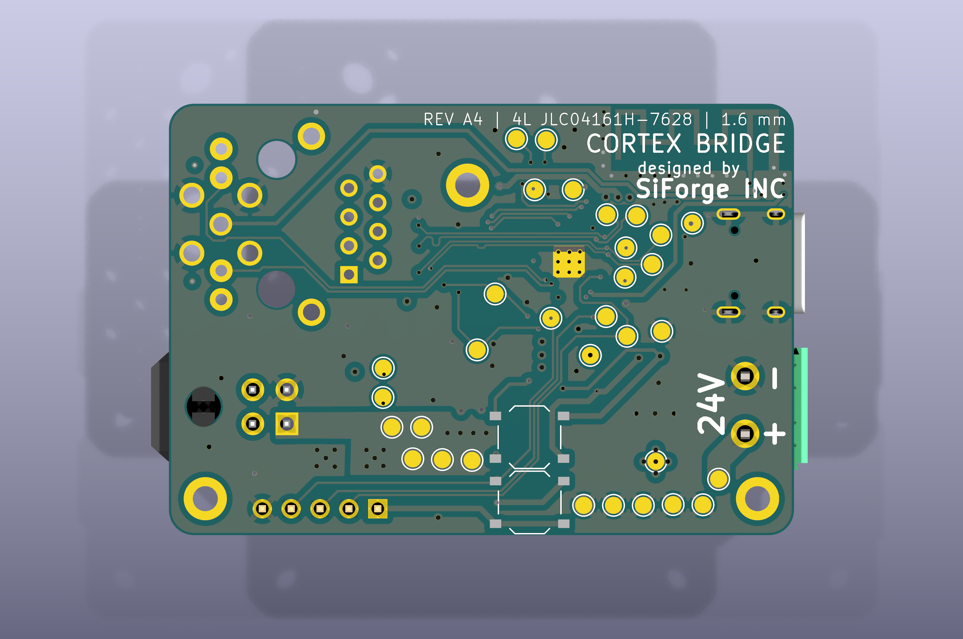
Underside. The "24V +/-" marking is at the power terminal. The board also carries the "REV A4" marking and the text "CORTEX BRIDGE / designed by SiForge INC".
Both images are renders of the standard (as-fitted) A4 build, not photographs. Open either one at full size to read the silkscreen.
¶ Connectors
| Designator | Silkscreen | Type | Connects to | Used during installation? |
|---|---|---|---|---|
| J1 | USB-C | USB-C receptacle, USB 2.0 device port | Klipper host (Raspberry Pi or other Linux computer) | Yes |
| P1 | PWR IN | 2-position 5.08 mm screw terminal | Spare +24 V and 0 V terminals on the printer's 24 V power supply (or a separate 24 V DC supply) | Yes |
| CN1 | BUFFER | 4-pin, 3.0 mm pitch, 2x2 through-hole wire-to-board connector (Micro-Fit 3.0 style) | AMS filament buffer sensor connector, by the 4-pin Molex cable | Yes |
| J4 | PRGRM | Molex PicoBlade 1.25 mm, 6-pin, right-angle SMD | Nothing; not used | No |
| J7 | CH32 DEBUG | 5-pin 2.54 mm header | Service and debug use only | No |
| J5 | (10BASE-T outline) | RJ45 jack, optional | Not fitted | No |
P1 pins
| Pin | Signal |
|---|---|
| 1 | +24 V raw input |
| 2 | GND |
CN1 pins
| Pin | Signal |
|---|---|
| 1 | +24 V protected output |
| 2 | GND |
| 3 | RS485 P |
| 4 | RS485 N |
These are connector pin numbers, not a left-to-right viewing order. Do not read the pin order from the render.
¶ Power
The bridge has two separate power inputs. USB powers the bridge logic. 24 V, taken from spare terminals on the printer's own 24 V power supply, feeds the AMS network. Both must be connected. The supply needs spare capacity for the AMS units, which draw the most while drying; check it against drying, not idle.
¶ 24 V path to the AMS
P1 → F1 (5 A fuse) → Q1 (reverse-polarity stage) → CN1 pin 1
D7 clamps the fused input and D5 clamps the protected output. Both sit across the rail, not in series with it.
- F1 is a 5 A very-fast fuse. It opens if the board or the cable draws too much current.
- D7 is a 28 V bidirectional TVS diode on the fused input. It clamps voltage spikes on the supply, whichever polarity they have.
- Q1 is a P-channel MOSFET that blocks current if the supply is connected the wrong way round. D6, a 12 V clamp, protects its gate.
- D5 is a 28 V TVS diode on the protected output. It clamps spikes that reach the AMS side.
¶ USB logic power
J1 (USB 5 V) → Q3 → U6 (3.3 V regulator) → +3V3 rail
- U4 is a USBLC6-2SC6. It protects the USB D+ and D- lines against electrostatic discharge.
- Q3 is a P-channel switch between USB 5 V and the regulator input. It is on in normal use. SW2 would switch it off for a power-cycle reset, but SW2 is not fitted.
- U6 is an AMS1117-3.3 regulator. Its output is the 3.3 V logic rail.
Without USB, the logic does not run, even if 24 V is present. Without 24 V, the bridge can enumerate on USB, but the AMS network has no power.
¶ Status LEDs
A4 added these three LEDs. A3 had none.
| LED | Colour | On means | If it stays off |
|---|---|---|---|
| D8 | Red | The protected 24 V output is present | 24 V is not reaching the output. Check the P1 wiring and polarity. Measure TP22, TP23 and TP24. |
| D9 | White | USB 5 V is present | The USB cable or host port is not supplying 5 V. Measure TP8. |
| D10 | Green | The 3.3 V logic rail is present | The regulator is not producing 3.3 V. Check that D9 is on, then measure TP1. |
¶ Main chips
- U1, CH32V208GBU6: the main microcontroller. WCH QingKe V4C RISC-V core, 144 MHz, 128 KB flash, 64 KB SRAM, dual USB full-speed, BLE 5 radio.
- Y1: 32 MHz crystal for U1.
- U3, THVD1450DR: 3.3 V half-duplex RS-485 transceiver. It drives the AMS network lines (RS485 P and N).
- U4, USBLC6-2SC6: USB ESD protection.
- U5, ATECC608B: secure crypto coprocessor on the microcontroller's I2C bus.
¶ Radio
ANT1 is a printed inverted-F antenna (TI SWRA117D) on the top-right edge of the board. It serves the BLE radio in U1. L1 (1.8 nH) is a matching part for the BLE production variant. BLE is not used by the AMS connection.
The RF1 SMA connector is a test connector for RF measurements. It is not fitted in the standard build. Its signal path and the PCB antenna are mutually exclusive.
¶ Headers, pads and test points
J4 (PRGRM). Not used. Leave it unconnected.
Q2. Q2 switches power to J4. It is off in normal use.
J7 (CH32 DEBUG). J7 is a service and debug header with five pins: 3V3, BOOT0, SWCLK, SWDIO and GND. It is not part of the installation.
SW1 and SW2. SW1 ("BOOT / USB ISP") and SW2 ("RESET / POWER CYCLE") are tactile-switch pads on the underside. They are not fitted. Unplugging USB does the same job as SW2.
Test points. The board has test points TP1 to TP34. These are the useful rail checks.
| Test point | Net | Should read |
|---|---|---|
| TP22 | Raw 24 V input | About 24 V |
| TP23 | Fused 24 V | About 24 V |
| TP24 | Protected 24 V output | About 24 V |
| TP8 | USB VBUS | About 5 V |
| TP1 | +3V3 | About 3.3 V |
¶ Not fitted in the standard build
- The J5 10BASE-T Ethernet jack and its support parts. The silkscreen outline and pads are on the board but unpopulated.
- The RF1 SMA connector.
- SW1 and SW2.
The board lives in a printed case on the printer's rear panel: Print and mount the case.
Next: Quick start.